Congratulations to Jessica and the rest of the team on publishing the 4D-STEM paper in Nano Letters.

The directed assembly of nanoscale building blocks into complex superstructures is of widespread scientific and technological interest. Scientists and engineers have been intrigued by the prospects of tailoring self-assembly processes to create materials whose properties and function can be tuned through the interaction between constituent particles. In particular, recent reports of superlattice structure transformations leading to epitaxially connected nanocrystal superlattices with long-range atomic coherence have generated significant interest as a platform for novel, quasi 2D ‘designer materials’. Although experimental protocols for the formation of high quality superlattices in which constituent nanocrystals are registered to within a single atomic bond length have been established, significant gaps persist in our fundamental understanding of several aspects of the underlying mechanism by which these structures form.

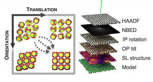
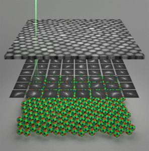
In this article, we apply advanced electron diffraction to investigate the superlattice transformation of lead chalcogenide (PbX, X=S, Se) nanocrystals leading up to 2D oriented attachment. We present unprecedented detail into the exact position and 3D crystallographic alignment of each polyhedral NC in the assembly derived from nanobeam electron diffraction pattern maps acquired with an electron microscope pixel array detector (EMPAD). This analysis reveals that the nanocrystals are strongly coupled along the <11n>AL direction and undergo translation with nearly constant in-plane atomic lattice orientation throughout the transformation. The rich experimental results presented here provide new mechanistic insights into the self-assembly and oriented attachment.

